


Ads by Google


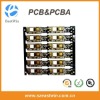
Rigid multilayer 4 Layer PCB prototype
PCB process capability:1.Layer: 2-22 layer2.Product type: Rigid PCB,High Density Inverter PCB,thick copper PCB3.Materials: FR-4, CEM-3, Teflon, Aluminum Substrate, Rogers, Halogen Free, High Tg 4.Copper Thickness: 140micron(4oz)5.Min Board Thickness: 0.4mm6.Max Board Thickness: 5.0mm7.Min finished Hole Diameter: 0.1mm8.Outer layer line width / spacing: 0.1mm/0.1mm9.Inner layer line width / spacing: 0.1mm/0.1mm10.Min aperture: 0.2mm11.Min Laser drilling: 0.1mm12.Min Ring Width: 0.11mm13.Min BGA-bit hole spacing: 0.4mm14.Resistance Tolerance: ±10%15.Minimum Insulation Thickness: 3mil16.Maximum laser blind hole thickness to diameter ratio: 0.8:117.Maximum working board size: 520*622mm18.Drilling Tolerance (PTH): ±0.075mm19.Drilling tolerance (NPTH): ±0.05mm20.Outline Tolerance (CNC): ±0.13mm21.Surface coating: Lead Free HAL, HAL, Flash Gold, Immersion Gold, Immersion Tin, Immersion Silver, OSP, Gold Finger Plating, Carbon Ink Printing, Peelable Blue Mask
Your single point of contact for all of your raw materials, parts, and pcb assembly, also offers: - Contract Manufacturing- Engineering Services- PCB Design & Assembly- Product Design- Prototyping- Cable and Wire Assemblies- Plastics and Molds
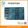
Detailed Terms for Pcb Assembly
Technical requirement:1) Professional Surface-mounting and Through-hole soldering Technology2) Various sizes like 1206,0805,0603 components SMT technology3) ICT(In Circuit Test),FCT(Functional Circuit Test) technology.4) PCB Assembly With UL,CE,FCC,Rohs Approval5) Nitrogen gas reflow soldering technology for SMT.6) High Standard SMT&Solder Assembly Line7) High density interconnected board placement technology capacity.
Quote requirement:1)Gerber file and Bom list2)Clear pics of pcba or pcba sample for us3)Test method for PCBA
Factory View:
All of the above description is to demonstrate the ability of our factory, if you have specific requirements, please contact us!