

Ads by Google


Printed circuit,RoHS PCB,PCB UL.
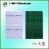
Quick Details
1.Place of Origin : Shenzhen China (Mainland)
2.Brand name: T-soar
3.Model Number : Ts102
4.Base Meterial : FR-4, CEM-3
5.Copper Thickness : 1.5oz
6.Board Thickness : 0.8-3.2mm
7.Min.Hole Size : 0.2mm
8.Min.Line Width : 4mil
9.Min.Line Spacing : 4mil
10.Surface Finishing : immersion gold,Gold Plating,Entek Coating OSP ,immersion silver
11.Certification : UL,ROSH,ISO9001:2000
12.Colour : blue
We offer quality PCB board with fast delivery and competitive price. We are here to assist to your success.
UL RoHS standard.
We are professional manufacture of PCBs of various kinds in Shenzhen ,China.
1.Our product range
Single PCB, Double PCB,Multi-layer PCB,MCPCB,High frequency PCB and Metal-backed PCB,etc.
2.Product quality
Our products got ISO and UL certificates and meet RoHS standard.
3.How can we help you.
What we offer is better solutions to help you improve your quality while maintaining low production
cost but not just products.
Our factory fabirc capacity:
NO | Item | Craft Capacity |
1 | Layer | 1-30 Layers |
2 | Base Material for PCB | FR4, CEM-1, TACONIC, Aluminium, High Tg MaterialHigh FrequenceROGERS ,TEFLON, ARLON, Halogen-free Material |
3 | Rang of finish baords Thickness | 0.21-7.0mm |
4 | Max size of finish board | 900MM*900MM |
5 | Minimum Linewidth | 3mil (0.075mm) |
6 | Minimum Line space | 3mil (0.075mm) |
7 | Min space between pad to pad | 3mil (0.075mm) |
8 | Minimum hole diameter | 0.10 mm |
9 | Min bonding pad diameter | 10mil |
10 | Max proportion of drilling hole and board thickness | 1:12.5 |
11 | Minimum linewidth of Idents | 4mil |
12 | Min Height of Idents | 25mil |
13 | Finishing Treatment | HASL (Tin-Lead Free), ENIG(Immersion Gold), Immersion Silver , Gold Plating (Flash Gold), OSP, etc. |
14 | Soldermask | Green, White, Red, Yellow, Black, Blue, transparent photosensitive soldermask, Strippable soldermask. |
15 | Minimun thickness of soldermask | 10um |
16 | Color of silk-screen | White, Black, Yellow ect. |
17 | E-Testing | 100% E-Testing (High Voltage Testing); Flying Probe Testing |
18 | Other test | ImpedanceTesting,Resistance Testing, Microsection etc., |
19 | Date file format | GERBER FILE and DRILLING FILE, PROTEL SERIES, PADS2000 SERIES, Powerpcb SERIES, ODB++ |
20 | Special technological requirement | Blind & Buried Vias and High Thickness copper |
21 | Thickness of Copper | 0.5-14oz (18-490um) |
This is our website: www.tsoar-pcb.com