


Ads by Google

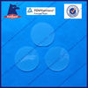

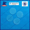
Sapphire wafer
Worldhawk offers a series wafer with different materials. Sapphire is a material of a unique combination of physical, chemical and optical properties, which make it resistant to high temperature, thermal shock, water and sand erosion, and scratching. It is a superior window material for many IR applications from 3µm to 5µm. C-plane sapphire substrates are widely used to grow III-V and II-VI compounds such as GaN for blue LED and laser diodes, while R-plane sapphire substrates are used for the hetero-epitaxial deposition of silicon for microelectronic IC applications.
Product Description
| crystal materials | 99.996% high purity monocrystalline AL2O3 | |||
| wafer surface orientation | C-axis(0001)to M(1-100)or A(11-20)0.2°+/-0.1° | |||
| Dia | 50.8+/0.1mm | 76.2+/-0.25mm | 100.0+/-0.2mm | 150.0+/-0.5mm |
| thickness | 430+/-25um 330+/-25um | 650+/-25um 430+/-25um | 650+/-25um 550+/-25um | 1000+/-25um |
| Major Flat | A-axis(11-20)+/-0.2° | |||
| Major Flat Length | 16.0+/-1.0mm | 22.0+/-1.0mm | 31.0+/-1.0mm | 57.0+/-1.0mm |
| Front surface | Epi polished, Ra<0.20nm | |||
| Back Surface | Fine ground(Ra=1.0um)or Epi-polished,Ra<0.20nm | |||
| Edge condition | small protective chamfer | |||
| TTV | ≤5um | ≤5um | ≤5um | ≤5um |
| BOW | ≤5um | ≤7um | ≤10um | ≤15um |
| Warp | ≤5um | ≤7um | ≤10um | ≤15um |
| surface quality | Epi-ready | |||
| packaging | packaged in class 100 clean room evnvironment, in cassettes of 25pcs or single package ,under in nitrogen atomosphere | |||
| Note | R-pane(1-102),A-plane(1 1-20)and M-plane(1-100)are available | |||
Our main products include optical components, laser products, Lenses assembly and other electronics devices, if any other needs, please feel free to contact with us. We will supply our best service for you!